
Excerpt from Understanding Personal Computer Hardware by Steven Roman, published by Springer-Verlag. ISBN: 0-387-98531-X.
Copyright © 1999 by The Roman Press, Inc. All Rights Reserved. You may view and print this document for your own personal use only. No portion of this document may be sold or incorporated into any other document for any reason.
Memory
The purpose of memory is to store information in a manner that allows as rapid reading and writing as possible. These days, a modern computer usually has between 16 MB and 128 MB of memory, which is enough to store between 2000 and 16,000 pages of single-spaced text. On the other hand, it may not be enough to store a large, full color photograph.
Memory stores bits using electric charges. These charges need a constant power supply to remain valid. Thus, as we have mentioned, all data in memory is lost when the computer is turned off and the current is removed. In short, memory is fast, temporary storage.
Figure 8.1 shows a typical memory chip, in actual size. The memory chip itself is a small sliver of silicon no bigger than a fingernail. However, since it is so sensitive to air that exposure would destroy it, the chip is hermetically sealed in a plastic case, as shown in the figure. The larger size of the case also provides enough room for the pins.
Memory chips are generally placed in computers in memory banks consisting of 8 or 9 chips per bank. In early PC systems, adding additional memory required carefully inserting these chips, one by one, into sockets on the motherboard or on a memory expansion board. If a fragile pin was bent, it could easily break, rendering the chip useless.
These days, most PCs are designed to accept packages of chips that are permanently soldered onto their own small circuit boards. The most popular version of this is the single inline memory module, or SIMM, shown in Figure 8.2. SIMMs are much easier to install and remove than individual chips.
Figure 8.1 - A computer memory chip (actual size)
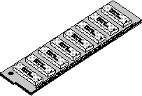
Figure 8.2 - A SIMM package
One edge of the SIMM board has the metal contacts that take the place of pins. This edge snaps easily into a SIMM socket, eliminating the problem of breaking a pin. Thus, SIMMs are much easier to install and remove than individual memory chips, bringing the process of upgrading memory into the realm of the average user. Figure 8.3 shows how the letter E (as an ASCII codeword) might be stored in a SIMM module inside a PC.
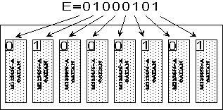
Figure 8.3 - The letter E in memory
Data in main memory is arranged in such a way that any portion of memory can be directly read or written, without having to wade through other portions of memory. This is referred to as random access. Accordingly, memory of this type is referred to as random access memory, or RAM. Data on a tape, for instance, is not random access, for it is not possible to access data in the middle of the tape without going through the beginning of the tape first. Thus, tape is said to be a sequential access medium.
The most common, and least expensive, type of memory uses a tiny capacitor to hold an electric charge that represents a bit of information. (A capacitor is simply a device that is designed to hold an electric charge.) The presence of a charge indicates a 1 and the absence of a charge indicates a 0, or vice versa, depending upon the manufacturer of the chip. Unfortunately, a capacitor can only hold a charge for a very brief time and so it must constantly be refreshed. For this reason, this type of RAM is called dynamic RAM, or DRAM.
A faster, and more expensive, type of memory uses very tiny switches, called flip-flops, to hold the value of a bit. Flip-flops are stable, that is, they hold their position until a new current is applied, and so refreshing is not required for this type of memory. RAM that does not require refreshing is called static RAM, or SRAM. Unfortunately, SRAM is too expensive to use in main memory, but its increased speed (approximately 3-5 times faster than DRAM) makes it very useful for relatively small level 2 cache memory.
As we mentioned, when the current is removed from memory (either DRAM or SRAM), all information is lost. However, it is possible to design memory that does not loose data when the current is turned off. Read-only memory, or ROM, is memory that is designed to hold data persistently, that is, after power has been removed. The information in early ROM chips was literally burned into the chip, making the data truly permanent, but later technologies have allowed data to be stored persistently but not permanently, as we shall see.
ROM memory is used in a PC for a variety of specific purposes. For instance the system BIOS is stored in a ROM chip, hence the name ROM BIOS. Also, the device BIOS on an adaptor card is stored in ROM chips. ROM is used inside the Pentium microprocessor to hold the microcode that we discussed earlier.
Note that there is a potential for some confusion in terminology here, since RAM stands for random access memory, but ROM is also random access. By common usage, the distinction between RAM and ROM is that RAM can be written to, but ROM cannot (at least not easily or repeatedly).
There are a variety of different strategies for making ROM chips. Let us review some of the more common ones.
One form of ROM chip is called a programmable ROM, or PROM, chip. The circuits in a PROM consist of small fuses. Initially, all fuses are in tact, allowing current to flow freely. The programmer of the PROM melts some of the fuses, using a strong current, to determine the operating characteristics of the PROM chip. This process is called burning a PROM. Once the PROM is burned, its information is completely determined. This is truly permanent storage.
It is now possible to design an erasable programmable ROM chip, or EPROM. In such a chip, a strong ultraviolet light can restore the links broken by burning the chip. EPROMs can be recognized by a small window in the middle of the chip's package, to allow the light to reach the chip. (The window is covered by a label for protection from unwanted light.) Incidentally, ordinary room light is not generally sufficient to erase an EPROM, but sunlight can be!
Electrically erasable programmable ROM, or EEPROM, is ROM that can be erased using an exceptionally strong current, rather than ultraviolet light. This has the distinct advantage that the chip does not have to be removed from the computer to erase it. However, the current form of EEPROM can only be erased a modest number of times, and the entire contents of the chip must be erased at one time-it is all or nothing. Thus, EEPROMs are not a suitable replacement for RAM.
The latest wrinkle in the ROM saga is flash RAM. This is like EEPROM, but can be erased using ordinary levels of current. Flash RAM has found its way into the system BIOS of many modern PCs, as well as into the ROM BIOS of many peripheral devices, such as modems. It still suffers from the drawbacks of EEPROM, however, and so does not provide a substitute for ordinary RAM. Incidentally, when shopping for a peripheral device for a computer, it pays to consider whether or not the device uses a flash RAM BIOS, for this will make it possible to easily upgrade the BIOS if new versions appear, or bugs are fixed. This is certainly far superior to replacing the chip itself.
The permanence of ROM carries with it some interesting consequences, stemming from the fact that nothing is perfect. For instance, early IBM PCs suffered from a certain bug in their system BIOS that affected certain types of software. (It is probably safe to say that all system BIOS's have bugs.) This raised an interesting dilemma to software manufacturers. Should a software company deliberately alter their software, in effect introducing a deliberate bug, in order to compensate for a bug in the system BIOS? What if the next version of the BIOS no longer has the bug? Then the software will no longer run and it will appear to customers that this is due to a gratuitous bug on the part of the software company! On the other hand, if the software is not altered, it certainly will not sell, since it will not work with the defective BIOS.
As we will see when we discuss the video system of a PC, video images are formed in a special type of memory that resides on the video adaptor card, before being displayed. Special circuitry constantly moves the memory image to the monitor, translating the digital data into the analog signals required by the monitor. This typically happens 60-80 times per second. At the same time, whenever the image changes, which may be many times per second, the CPU needs to have access to the video memory to make the necessary changes. Thus, the same location in video memory may need to be accessed at the same time by two different sources. Since ordinary DRAM cannot be read from and written to at the same time, either the CPU or the display would have to wait. This may produce delays in the display of images.
Low performance video adaptors often use DRAM for video memory, but higher performance adaptors use a special type of memory known as VRAM. A VRAM chip has two separate data paths for each bit. One path can be used for both reading and writing bits. This is the path used by the CPU. The other path is read-only and is used to refresh the image on the display. Thus, both processes can take place at the same time. This two-way design is often called dual-ported memory.
Memory chips come in different speeds. The access speed of a memory chip is the time between the presenting of an address to the chip and the time that the data is ready for output from the chip. The cycle time is the shortest time between successive requests for data from the chip. For DRAM chips, the cycle time is the access time plus some additional time it takes for the circuits inside the chip to prepare for the next request. This often means that the cycle time is 2 or 3 times the access time. SRAM chips do not need such preparations, and so the cycle time is the same as the access time. This is one reason why SRAM chips are faster than DRAM chips.
Most DRAM access speeds are in the range of 60-80 ns (billionths of a second). This means that a single request for data from a chip can be honored in 60-80 billionths of a second.
SRAM chips have access times in the 15-20 ns range. On the other hand, EPROMs have access times in the 120-250 ns range, and are thus slow relative to RAM. This is why many modern computers offer the option of moving important ROM BIOS code, such as video or system BIOS, from ROM to faster RAM, a process known as shadowing ROM. (The area of RAM that stores the code is called shadow RAM.)
Some SIMM packages have an extra chip that is used for parity checking. The purpose of parity checking is to detect errors that may occur when data is read. The principle of parity checking is extremely simple. To each byte (8 bits), we associate an extra bit, called an even parity check bit. This parity check bit is chosen so that there are always an even number of 1's in the 9 bits. Thus, if the byte already has an even number of 1's, the parity check bit is a 0, but if the byte has an odd number of 1's, the parity check bit is a 1. For instance, the ASCII code for E is 01000101 and since this has an odd number of 1's, the parity check bit is a 1 (bringing the total number of 1s to 4, which is even).
Figure 8.4 illustrates a SIMM with an even parity check chip. Now, here is the point. If a glitch should occur and exactly one of the 9 bits were to be altered, then there would be an odd number of 1's in those 9 bits. When the computer reads these 9 bits, it does a quick parity check and discovers that there are an odd number of 1's. This results in a parity check error. The user will then get a nasty error message. Repeated parity errors require that the SIMM be replaced. Fortunately, modern memory is generally quite reliable, and you may never encounter a parity check error.

Figure 8.4 - SIMM with parity chip
Note that the manufacturer of the computer decides whether or not to support parity checking. If a PC supports parity checking, all SIMMs inserted into that PC must have parity check support.
Note also that parity checking can detect the presence of any odd number of errors, because this will result in an incorrect parity. However, any even number of errors will go undetected. We should also emphasize that parity checking can only detect errors. There are other, more sophisticated approaches that can not only detect single errors, but also correct them! This technology is available in some PCs, and is referred to as error-correcting code, or ECC.
Memory SIMMs are packaged in a variety of ways. From the consumer's point of view, the issues that matter are
· The capacity of the SIMM, usually measured in megabytes,
· The number of pins on the SIMM,
· Whether or not the SIMM supports parity checking.
SIMM Capacity
The capacity of a SIMM refers, of course, to the amount of data that the SIMM can hold. SIMMs come in a variety of capacities, commonly ranging from 2 MB to 32 MB.
One important practical issue related to SIMM capacity stems from the limited number of SIMM slots on a PC motherboard. The number is usually 4 or 6. Consider a PC with only 4 SIMM slots. If you purchase such a PC with 16 MB of RAM, the dealer may install four 4-MB SIMMs, since it may be cheaper than installing two 8-MB SIMMs. This will fill up all of the SIMM slots, which is bad news if you later decide to add more memory.
For instance, on a Pentium PC, which requires that SIMMs be installed in matching pairs (we will see why in a moment), to add an additional 8 MB, you will need to remove two 4-MB SIMMs and replace them with two 8-MB SIMMs. To add 16 MB, you would need to replace all four 4-MB SIMMs! This is a major waste of chips and money.
Thus, when buying a PC, look for a motherboard with 6 SIMM slots or, failing that, make certain that the dealer installs the smallest number of SIMMs that will give you the desired memory-in this case two 8-MB SIMMs. This will leave you free to upgrade without throwing away perfectly good memory.
SIMM Pin Count
The pins (actually metal tabs) on the bottom edge of a SIMM slip into the SIMM slots on the motherboard. There are two common pin counts on SIMMs. Of course, the number of data pins on the SIMM must match the data bus width. However, a SIMM needs more than just data pins, so the pin count is larger than the data width. In fact, SIMMs designed for an 8-bit data bus have 30 pins and SIMMs designed for a 32-bit data bus have 72 pins. However, since a modern Pentium PC has a 64-bit wide data bus, 72-pin SIMMs must be installed in pairs in these PCs. (Some older Pentiums have 32-bit data buses.)
SIMM Labeling
The labeling that memory sellers use to describe SIMM chips can be a bit confusing. A SIMM is often labeled using the following format:
SIMM depth in Megs × Data width (including parity) in bits - Pin count
To explain this format, we need to explain the SIMM depth. This is simply the number you need to multiply by the data width, not including parity, to get the SIMM's capacity.
For example, an (8×32-72) SIMM has 72 pins, a data width of 32 bits (that is, 8 bytes), does not use parity, and has a SIMM depth of 8 megs. Hence, its capacity is
Capacity = 8 Megs × 32 bits = 32 MB
As another example, a (4×36-72) SIMM has 72 pins, 32 data bits (that is, 8 data bytes) plus 4 more bits for parity and a SIMM depth of 4 megs. The capacity is thus
Capacity = 4 Megs × 32 bits = 16 MB
SIMM Chip Count
It can be a bit of a surprise to buy a new SIMM for a PC and find that, while all the previously installed SIMMs in your PC have 8 chips, the new SIMM has only 2 chips! Actually, it is possible to reach a given capacity in a variety of ways that involve a different number of chips on the SIMM. Sometimes, it is less expensive for the manufacturer to use fewer chips each having a larger individual capacity. (My PC presently houses 4 SIMMs with 8 data chips each and 2 SIMMs with 2 data chips each.) The details on which chip combinations are possible are a bit involved, and so we will save them for an appendix.
Chip Labeling
Each memory chip is stamped with a label to indicate its properties. There are occasions when it is useful to understand at least a portion of this labeling. Here is an example of how the chip manufacturer Micron Technology labels their chips:
MT4LC1M16E5TG-7
The important items to note here are the characters 1M16 (underlined by me for clarity) and the -7 (at the end). The former denotes the dimensions of the chip, which in this case is 1 Meg by 16; that is, the chip has a width of 16 bits and a depth of 1 Meg, for a total capacity of 16 megabits. (Chip width and depth are further explained in the appendix, in the discussion of SIMM chip counts.) Thus, 2 of these chips on a single SIMM board would produce a 1×32 SIMM with capacity 4 MB.
The last digit (following the hyphen) refers to the speed of the chip. By appending a 0 to the end, we get 70 ns. Unfortunately, labeling varies among chips and among manufacturers, but at least this gives you something to work from if you ever want to read a chip label.
The story of how a memory chip actually works is a fascinating one. However, since it is a bit involved, we have placed it in an appendix. If you are curious, by all means take a look at that appendix now.
Let us turn now from the physical layout of memory to its logical layout.
The address space of a PC can be divided into three logical parts-conventional memory, upper memory and extended memory-as shown in the memory map in Figure 8.5. Note that this is a logical division; that is, a division based on how the memory is used. Note also that, as previously mentioned, not all of this address space need be populated with actual memory chips.

Figure 8.5 - A memory map
Conventional Memory
The first 640 KB of memory space is called conventional memory. The first 1024 bytes of conventional memory is used for the interrupt vector table, discussed in a previous chapter. The next 256 bytes is used for the BIOS data area, which we also discussed earlier. The DOS operating system then occupies some memory, generally between 20 KB and 90 KB, depending upon how the system is configured (a task usually left up to the user, by the way). Next comes various software drivers (mouse, sound card, etc.). Finally, the remainder of conventional memory (between about 450 KB to 620 KB) is free to be used by applications-both DOS and Windows based. In fact, conventional memory was the only available memory for the first 8088-based PCs.
Note that 450 MB of conventional memory is not sufficient for many applications, a problem that can be addressed by loading some software in upper memory, as described next.
Upper Memory
The next portion of memory, called upper memory, is filled in a rather eclectic way. It is generally used by hardware adaptor cards, such as video and hard disk controllers, for their device BIOS code. Thus, there is usually no physical memory on the motherboard corresponding to these addresses. But, for example, the BIOS on a video card is assigned addresses in this range. We have already discussed some of the problems that may arise with memory conflicts in this address range.
It is also often the case that some portions of upper memory are not being used. When this happens, it may be possible to move some of the operating system files and device drivers that normally place themselves in conventional memory into free "holes" in the address space of upper memory. This is referred to as loading software in upper memory. Free blocks of upper memory are called upper memory blocks, or UMBs. Note that actual physical memory must be borrowed from what would otherwise be used by running applications (extended memory) in order to populate upper memory.
High Memory
There is also a very small portion of memory addresses (a little less than 64 KB) that is always available to DOS-based programs running under all processors except the 8088. It is located immediately above the 1 MB range and called the high memory area, or HMA. It is thus often possible to load software in high memory, helping to free up as much of the 640 KB of conventional memory as possible.
If you are curious about where the HMA came from, here is the story. You can skip this discussion if desired.
As we have seen, the 8088 has a 20 bit address bus, allowing for a 220 = 1 Meg address space. The linear address range is thus 0 to 220-1 = FFFFFh. However, the 8088 registers are only 16 bits wide. For this reason, addresses are generally expressed in segmented form. We will discuss this form in detail in the appendix on real and protected mode. Suffice it to say for now that segmented addresses are usually written in the form segment:offset. For example, FFFF:0000 is an address in segment:offset form. Each portion (segment and offset) fits nicely into a 16-bit register.
To convert a segmented address to a linear address, simply put a 0 on the right end of the segment and add the offset to the resulting number, as follows:
FFFF:0000 = FFFF0 + 0000 = FFFF0
Now, observe that the address (in segment:offset format) that corresponds to the very last linear address that the 8088 can reach (FFFFF) is FFFF:000F, since
FFFF:000F = FFFF0 + 000F = FFFFF
Thus, because of the nature of the segment:offset scheme, the registers in an 8088 can store the addresses
FFFF:0010 = FFFF0 + 0010 = 100000h = 1,048,576 decimal = 1 meg
through
FFFF:FFFF = FFFF0 + FFFF = 10FFEFh = 1,114,095 decimal
which consists of 65,520 bytes of memory beyond the 1 MB range of the 8088.
In summary, the registers of the 8088, through the use of segmented address format, can recognize some addresses (64 KB minus 16 bytes) beyond what the actual address lines of the 8088 can access. These addresses cannot be physically addressed because the 8088 only has 20 physical address lines.
However, the 80286 and later processors have more than 20 address lines! Thus, when an 80286, for instance, is operating in real mode, which is designed to emulate the 8088, special circuitry in the chip is used to turn off the 21st address line (known as A20, since the first address line is A0). Thus, any attempt to address memory beyond 1 MB is defeated. (Actually, addresses starting at 1 MB and above are wrapped back around to 0.) However, by reactivating the A20 address line, the 80286 can physically access the roughly 64 KB address space that the 8088 cannot physically reach. This address space is the high memory area, or HMA.
Expanded Memory
It did not take long in the PCs history for DOS based programs to run into the 640 KB conventional memory barrier. This prompted some large software and hardware companies to join forces and come up with a method for allowing DOS to access more than 640 KB of memory without realizing it. This trick is called the expanded memory specification, or EMS (which should not be confused with extended memory). The idea behind EMS is relatively simple, but we cover it briefly, since it is no longer a major tool for increasing memory. These days, it is used primarily because some older applications were written to use it.
We should emphasize before beginning that expanded memory is a technique for increasing the effective address space of a PC. It is not a region of memory in the same sense as conventional, upper or extended memory.
To implement EMS, you need two things: a special memory board, called an EMS memory board, containing some physical memory; and a software program called an EMS memory manager, to manage the EMS process. It is also possible to devote some RAM to use in place of the EMS board, if you care to spare the RAM. Note that EMS will work only with applications designed to take advantage of it.
The EMS memory board is used as follows. A total of 64 KB of physical memory on the board is given addresses in a consecutive memory block of upper memory, called an EMS page frame. (See Figure 8.6.) Addresses in the page frame, being within the first 1 MB, are accessible even to an 8088 microprocessor. The rest of the memory on the EMS board is not directly accessible to the microprocessor. Now, if an EMS-aware program requests some data, the EMS memory manager checks to see if that data happens to lie in the page frame (an EMS page frame hit). If so, the program can retrieve the data. If not (an EMS page frame miss), the EMS manager finds it on the EMS expansion board and swaps it with data that is in the page frame. The swapping takes place in chunks of 16 KB. Once the swapping is complete, the program can access the data. Thus, in effect, the program has more memory than it thinks it does! (Note the resemblance to caching, but for a different purpose-caching is done for speed, EMS is to increase effective address space.)
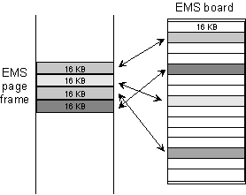
Figure 8.6 - The expanded memory specification (EMS)
Extended Memory
Extended memory refers to the memory addresses above the 1 MB range. Microsoft Windows and its applications are the primary users of extended memory. It is not uncommon for a computer system to have a total of 16-128 MB of memory. Thus, after taking into account the 640 KB of conventional memory, there is at least 15 MB for extended memory. Windows 3.1 requires the computer user to install an extended memory manager or EMM, called HIMEM, in order to take advantage of extended memory. However, Windows 95 and Windows NT have an extended memory manager built into the operating system.
If you speak much with hardware technical support personnel, sooner or later you may discuss memory addresses. Most computer experts(?) use hexadecimal numbers for addresses and speak in terms of upper memory address blocks, as shown in Figure 8.7. Note that each block is 64 KB long. They are knowingly referred to as the A block, B block, C block, and so on. I am not aware of any analogy with the blocks of a prison, however. As we will see, the A and B blocks, and often the first half of the C block, are reserved for video memory.

Figure 8.7 - Upper memory address blocks (64 KB each)
If you have been around computers for a while, there is a reasonable chance you have heard the terms real mode and protected mode.
In general terms, all microprocessors, starting with the 80286, can run in either real or protected mode. The main functional differences are that in real mode, the processor can only address the same 1 MB as the original 8088 processor (as well as the HMA discussed earlier, for 80286 and later processors). Moreover, a running application has access to all of this address space, and can thus, for example, overwrite a portion of memory that is currently being used by the operating system (DOS). This usually brings the system to a halt, called a system crash, and requires that the user hit the reset button (or turn off the power), loosing all currently unsaved data.
On the other hand, protected mode, which is used in a multitasking environment such as Microsoft Windows, is designed to prevent running applications from encroaching upon the memory reserved either for other running applications or for the operating system (Windows and/or DOS). Moreover, protected mode operation has a feature known as virtual memory management, which allows an application to think it has access to the entire 4 GB memory address space (for an 80386 and above)!
Real mode exists for the purposes of backward compatibility with the thousands of applications that have been written for this mode. When a PC is first started, it powers up in real mode. Microsoft Windows will switch the processor into protected mode.
Readers who are interested in more details about real and protected mode will find an appendix on the subject at the back of the book.
Virtual 8086 mode was introduced in the 80386 in order to allow multiple DOS sessions. DOS applications cannot run in protected mode, since they do not understand the addressing scheme. On the other hand, real mode offers no memory protection. Thus, a new mode was created that uses the addressing scheme of real mode but some of the safeguards of protected mode.
The main feature of Virtual 8086 mode is that it allows the processor to create multiple virtual machines, each of which appears to operate in real mode. Each virtual machine accesses 1 MB of memory using the real mode addressing scheme and can host a DOS session. Thus, multiple DOS sessions can be running at one time. Moreover, Virtual 86 mode allows the operating system to control the I/O operations of each virtual machine separately. Thus, for instance, each virtual machine has a virtual keyboard, virtual video memory, virtual parallel ports, and so on. In this way, the operations of each virtual machine can be kept separate, and the operating system can decide which machine currently has access to the real (physical) I/O facilities of the PC.